Choosing the Right Path to Build Real Skills
Read More
"Learn new skills on your terms—full-time, part-time, or weekends, available both online and offline."

Happy Trainees
Placed
Google Rating
Workshop Strength
We focus on practical VLSI training, immersing students in hands-on projects with industry-standard tools. Our experienced mentors ensures trainees master real-world applications. Our trainees excel in top tech companies, turning skills into careers.

What we value most

We emphasize hands-on experience, ensuring students gain real-world skills by working on industry-relevant projects with cutting-edge tools and technologies.

Our courses are designed to meet current industry demands, equipping trainees with the skills and knowledge needed to excel in their careers and secure top positions in the tech sector.

Our experienced mentors, with extensive industry backgrounds, provide personalized mentorship, guiding students through practical applications and helping them master both fundamental and advanced VLSI concepts.
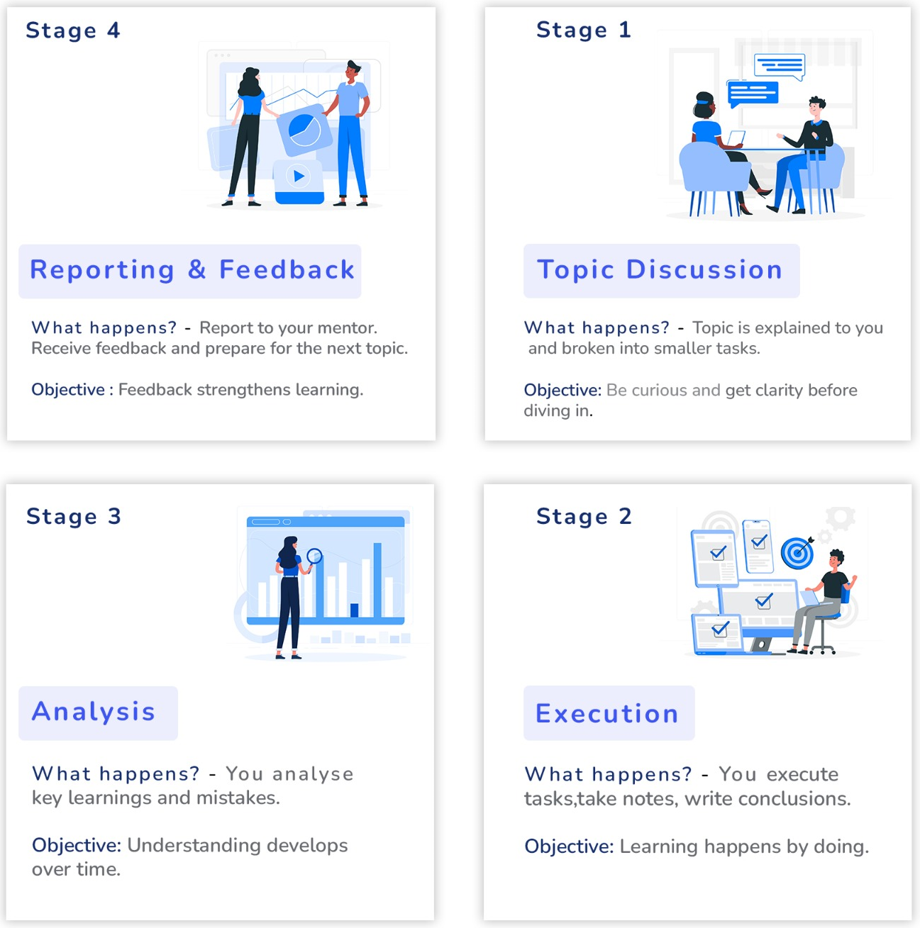
How 1 to 1 works?

Our Advanced Features

A genuine interest in the subject and a passion for learning drive students to explore beyond the curriculum and deepen their understanding.
The ability to keep going despite difficulties and a strong drive to achieve goals are essential, especially when tackling complex VLSI design problems that require sustained effort.
Strong analytical skills help in understanding intricate details, while critical thinking allows students to evaluate different solutions and approaches effectively.
Precision is vital in VLSI design, where even minor errors can lead to significant issues. Attention to detail ensures accuracy in design and implementation.
Working well in teams and communicating ideas clearly are essential for collaborative projects, peer learning, and professional interactions in the industry.
The ability to adapt to new technologies and methodologies and a commitment to continuous learning help students stay current in a rapidly evolving field like VLSI.
Check Our Courses
Physical Design is the process of place and route all the design components to meet area, power and performance requirements with out compromising on manufacturability. Most of the time these trade off decides the Quality of Results (QoR). As a Physical Design engineer we must handle these challenges effectivily to meet best QoR.
Read MoreSyntesis, is the process of converting design code in logic gates and optimizing for less area, less power and highest performance. On the other hand Sign-off STA (Static Timing Analysis) conforms on operating performance and data integrity.
Read MorePower Sign-off, is one of the imporant aspect of successful chip closure. Today's shrinking technology and battery operated devices poses a low power strategy with high reliability.
Read MorePhysical Verificaiton, is examining your design for all fabrication rules without which fab says no go for manufacturing. It has become to crutial at deep sub micron technologies as number of rules increases exponsially as technolgy node shrinks.
Read MoreASIC RTL Design, Developing architecture and coding of required functionality of the SOC (system-on-chip). The code should be synthesizable to gate level which later can be consider for ASIC development.
Read MoreVerification in VLSI ensures a design functions correctly by testing it against its specifications. Using simulations, testbenches, and formal methods, it identifies and corrects errors early in the design process. This critical step ensures the reliability and accuracy of semiconductor chips before manufacturing.
Read MoreFrequently Asked Questions
Classroom trainings are a thing of the past! If they were truly effective, you wouldn’t be here searching for skills. Instead, let's embrace a customized training approach—one that sparks curiosity, enhances engagement, and ensures a clear understanding of every concept. Studies show that when we are challenged, we learn up to ten times more effectively. So, let’s make learning an exciting and transformative experience!
Everyone can learn, but choosing the right platform is key to mastering skills, especially in the VLSI domain. Many institutes today focus on large batches, prioritizing quantity over quality. This approach leaves students with only theoretical knowledge and the ability to run a few scripts, but without the depth needed to excel. The lack of personalized attention often prevents learners from gaining the hands-on experience required to become industry-ready, leading to struggles in securing job placements. Our platform is different. We emphasize skill development through focused, personalized training. Every student gets the attention they need, ensuring that they are truly prepared for the VLSI industry and can confidently step into the workforce.
1. Research oriented approach 2. 1 on 1 Training from Industry Professionals 3. Personal mentorship and attention to each individual trainee 4. 24x7 tool access 5. Involve yourself in the work and you will evolve alongside the challenges you face
We’re not here to train you just for interviews—we’re here to help you build real skills from the ground up. Starting from the basics, our focus is on equipping you with the knowledge and hands-on experience that make you truly competent. With this strong foundation, you’ll naturally gain the confidence needed to face any interview and excel in your career. Let’s develop skills, not just answers.
What’s the point of training if it doesn’t lead to a job? That’s why our focus is simple: SKILL = JOB. We don’t just teach theory—we help you develop the practical, in-demand skills that employers are looking for. When you’re truly skilled, job opportunities follow. The right training is about preparing you for real-world challenges, ensuring that you’re not just interview-ready, but industry-ready. Build the skills, land the job.
Yes, we do offer online training. However, we strongly prefer and recommend offline training. Why? Because offline sessions provide a more immersive learning experience, with direct interaction, hands-on practice, and personalized guidance from trainers. This approach helps you grasp complex VLSI concepts better, ensures you get the attention you need, and allows for deeper skill development. Refer to our first answer for a more detailed explanation of why we prioritize offline training for effective learning outcomes.
Give us a call or send us a message on WhatsApp at +91 80 5062 3065. You can also Email us at info@iclabs.in
What they are saying about us
ICLabs is very good VLSI Training institute. I am very glad to join in this institute, I got very good practical knowledge. The trainer is very good and friendly in nature.

Right place to learn physical design course with good basics.Friendly environment and 24/7 tool access..more practical exposure with right guidance. Always available to clarify doubts.

It is good industrial training centre in Bangalore. I don't how to work on the EDA tools before joining here.after the training I got more knowledge on the industrial EDA tools and it is good institute.

"It’s one of the most practical learning institutions I have experienced. From Counseling to Placements assistance it provides end-to-end support for the candidates who are aspiring to get growth in the field of VLSI domain. Training is provided based on Industrial Projects and I got to learn the practical way of finding solutions. The interactive classes and the One-On-One Training helped the academic environment to be very friendly"

So, the journey began as my BTech in electrical and electronics was about to end. The pressure of career suddenly entered my mind as to what I should do after the BTech will be finished because, as you know, being in the core branch, you have very little option but to prepare for a government job or follow your passion. Then, I heard about a field called VLSI from my final-year mento. I sought to determine which institutions in India are the greatest because I was highly familiar with this field and Google did not provide any in-depth information.

Our hard working team


Our Trainees work at


Recent posts form our Blog
Contact Us
L149/A, 3rd Floor, 5th Main, 6th Sector
HSR Layout, Bangalore - 560102
+91 8050623065
info@iclabs.in
prasad@iclabs.in
Monday - Saturday
10:00AM - 08:00PM